


Solid-State LiDAR set for a revolution with Focal Plane Switch Array technology
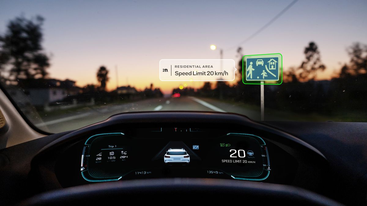
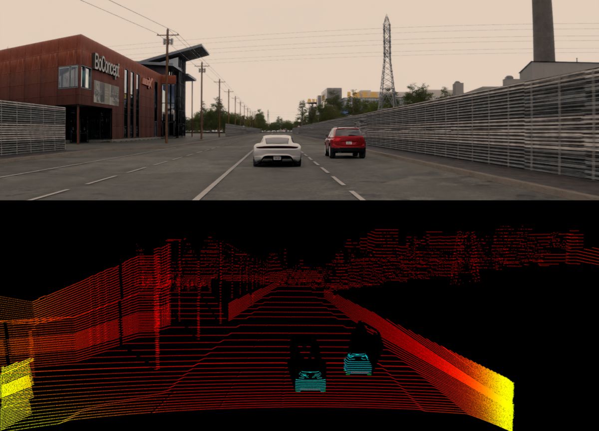
When Google unveiled its first autonomous cars in 2010, the spinning cylinder mounted on the roofs really stood out. It was the vehicle’s light detection and ranging (LiDAR) system, which worked like light-based radar. Together with cameras and radar, LiDAR mapped the environment to help these cars avoid obstacles and drive safely.
Since then, inexpensive, chip-based cameras and radar systems have moved into the mainstream for collision avoidance and autonomous highway driving. Yet, LiDAR navigation systems remain unwieldy mechanical devices that cost thousands of dollars.
That may be about to change, thanks to a new type of high-resolution LiDAR chip developed by Ming Wu, professor of electrical engineering and computer sciences and co-director of the Berkeley Sensor and Actuator Center at the University of California, Berkeley. The new design appears Wednesday, March 9, in the journal Nature.
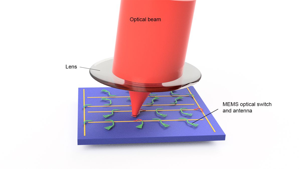
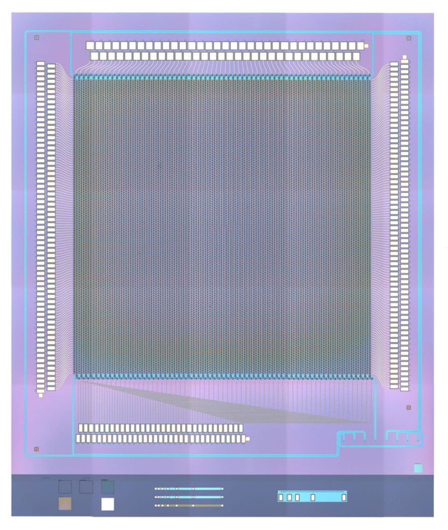
Wu’s LiDAR is based on a focal plane switch array (FPSA), a semiconductor-based matrix of micrometre-scale antennas that gathers light like the sensors found in digital cameras. Its resolution of 16,384 pixels may not sound impressive when compared to the millions of pixels found on smartphone cameras, but it dwarfs the 512 pixels or less found on FPSAs until now, Wu said.
Equally significant, the design is scalable to megapixel sizes using the same complementary metal-oxide-semiconductor (CMOS) technology used to produce computer processors, Wu said. This could lead to a new generation of powerful, low-cost 3D sensors for autonomous cars, as well as for drones, robots and even smartphones.
LiDAR barriers
LiDAR works by capturing reflections of light emitted by its laser. By measuring the time taken for light to return, or changes in beam frequency, LiDAR can map the environment and clock the speed of objects moving around it.
Mechanical LiDAR systems have powerful lasers that visualize objects hundreds of yards away, even in the dark. They also generate 3D maps with high enough resolution for a vehicle’s artificial intelligence to distinguish between vehicles, bicycles, pedestrians and other hazards.
Yet, putting these capabilities on a chip has stymied researchers for more than a decade. The most imposing barrier involves the laser.
“We want to illuminate a very large area,” Wu said. “But if we try to do that, the light becomes too weak to reach a sufficient distance. So, as a design trade-off to maintain light intensity, we reduce the areas that we illuminate with our laser light.”
That is where the FPSA comes in. It consists of a matrix of tiny optical transmitters, or antennas, and switches that rapidly turn them on and off. This way, it can channel all available laser power through a single antenna at a time.
MEMS switches
Switching, however, poses problems. Almost all silicon-based LiDAR systems use thermo-optic switches, which rely on large changes in temperature to produce small changes in the refractive index and bend and redirect laser light from one waveguide to another.
Thermo-optic switches, however, are both large and power-hungry. Jam too many onto a chip, and they will generate too much heat to operate properly. This is why existing FPSAs have been limited to 512 pixels or less.
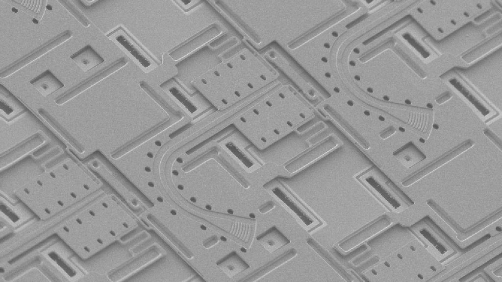
Wu’s solution replaces them with microelectromechanical system (MEMS) switches that physically move the waveguides from one position to another.
“The construction is very similar to a freeway exchange,” he said. “So, imagine you are a beam of light going from east to west. We can mechanically lower a ramp that will suddenly turn you 90 degrees, so that you are going from north to south.”
MEMS switches are a known technology used to route light in communications networks. This is the first time they have been applied to LiDAR. Compared with thermo-optic switches, they are much smaller, use far less power, switch faster and have very low light losses.
They are the reason Wu can cram 16,384 pixels on a 1-centimeter-square chip. When the switch turns on a pixel, it emits a laser beam and captures the reflected light. Each pixel is equivalent to 0.6 degrees of the array’s 70-degree field of view. By cycling rapidly through the array, Wu’s FPSA builds up a 3D picture of the world around it. Mounting several of them in a circular configuration would produce a 360-degree view around a vehicle.
Like smartphone cameras
Wu needs to increase FPSA resolution and range before his system is ready for commercialization. “While the optical antennas are hard to make smaller, the switches are still the largest components, and we think we can make them a lot smaller,” he said.
Wu also needs to increase the system’s range, which is only 10 meters. “We are certain we can get to 100 meters and believe we could get to 300 meters with continual improvement,” he said.
If he can, conventional CMOS production technology promises to make inexpensive chip-sized LiDAR part of our future.
“Just look at how we use cameras,” Wu said. “They’re embedded in vehicles, robots, vacuum cleaners, surveillance equipment, biometrics and doors. There will be so many more potential applications once we shrink LiDAR to the size of a smartphone camera.”
Other study co-authors include Xiaosheng Zhang, Kyungmok Kwon, Johannes Henriksson and Jianheng Luo of UC Berkeley.